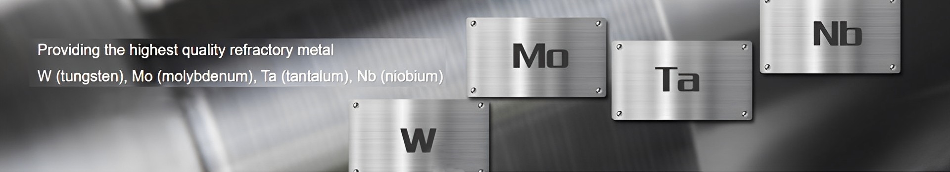

High-purity molybdenum target is one of the key raw materials in the production of AMOLED panels. The company’s new product is an ultra-wide, high-purity and high-density molybdenum planar sputtering target suitable for TFT-LCD / AMOLED. It is mainly used in G2.5-G6 generation TFT-LCD / AMOLED has filled the blank of the wide molybdenum target (1800mm), which will have an important impact on the company’s future market expansion and performance growth.
The requirements of sputtering targets are higher than those of the traditional materials industry. General requirements such as size, flatness, purity, various impurity content, density, N / O / C / S, grain size and defect control; higher requirements or special control Requirements include: surface roughness, resistance value, uniformity of grain size, uniformity of composition and structure, content and size of foreign matter (oxide), magnetic permeability, ultra-high density and ultra-fine grains, etc. Magnetron sputtering coating is a new type of physical vapor deposition coating method, which uses an electron gun system to emit and focus electrons on the material being plated, so that the sputtered atoms follow the principle of momentum conversion and fly away from the material with higher kinetic energy. A film is deposited on the substrate. This plated material is called a sputtering target. The sputtering targets are metals, alloys, ceramic compounds, and the like.
Magnetron sputtering coating is a new type of physical vapor deposition coating. Compared with evaporation coating, it has quite obvious advantages in many aspects. As a more mature technology that has been developed, magnetron sputtering has been applied to many fields.
Sputtering technology:
Sputtering is one of the main technologies for preparing thin film materials. It uses the ions generated by the ion source to accelerate the concentration in a vacuum to form a high-speed energy ion beam, which bombards the solid surface, and the ions exchange kinetic energy with the solid surface atoms. The atoms on the solid surface are separated from the solid and deposited on the surface of the substrate. The bombarded solid is the raw material for the sputtering method to deposit the thin film, which is called the sputtering target. Various types of sputtering thin film materials have been widely used in semiconductor integrated circuits, solar photovoltaics, recording media, flat displays, and surface coatings of workpieces.
Main application:
Sputtering targets are mainly used in the electronics and information industries, such as integrated circuits, information storage, liquid crystal displays, laser memories, electronic control devices, etc .; they can also be used in the field of glass coating; they can also be used in wear-resistant materials, high temperature and corrosion resistance , Decorative supplies and other industries.
Classification:
According to the shape, it can be divided into square target, round target and special-shaped target.
According to the composition, it can be divided into metal target, alloy target, ceramic compound target
According to different applications, it is divided into semiconductor-related ceramic targets, recording medium ceramic targets, display ceramic targets, superconducting ceramic targets, and giant magnetoresistive ceramic targets.
Divided into microelectronic target, magnetic recording target, optical disc target, precious metal target, thin film resistance target, conductive film target, surface modified target, photomask target, decorative target, Electric target, packaging target, other targets
Principle of magnetron sputtering: add an orthogonal magnetic field and electric field between the sputtered target (cathode) and yang, fill the required inert gas (usually Ar gas) in the high vacuum chamber, and the magnet is on the surface of the target material Form a magnetic field of 250-350 Gauss, and form an orthogonal electromagnetic field with the high-voltage electric field. Under the action of an electric field, Ar gas is ionized into positive ions and electrons. A certain negative high voltage is applied to the target. The electrons emitted from the target are affected by the magnetic field and the probability of ionization of the working gas is increased. A high-density plasma is formed near the cathode. Under the action of Lorentz force, Ar ions accelerate to fly to the target surface, and bombard the target surface at a high speed, so that the sputtered atoms on the target follow the principle of momentum conversion and fly away from the target surface to the base with higher kinetic energy. The sheets were deposited into a film. Magnetron sputtering is generally divided into two types: tributary sputtering and radio frequency sputtering. The principle of tributary sputtering equipment is simple. When sputtering metal, its rate is also fast. The use of RF sputtering is more extensive. In addition to sputtering conductive materials, non-conductive materials can also be sputtered. At the same time, reactive sputtering is also used to prepare compound materials such as oxides, nitrides, and carbides. If the frequency of radio frequency is increased, it will become microwave plasma sputtering. Electron cyclotron resonance (ECR) type microwave plasma sputtering is commonly used.
Post time: Jun-21-2023